Morning Edition · Tue 13 Oct 2026
Applied Materials Commits $5 Billion to Silicon Valley Chip R&D Center
Applied Materials on Monday unveiled its Equipment and Process Innovation and Commercialization (EPIC) Center in Sunnyvale, California, a $5 billion investment it calls the world's largest facility for collaborative chip-equipment and process R&D.
Chanan Zevin - Chief Editor and Head of Desks
Published
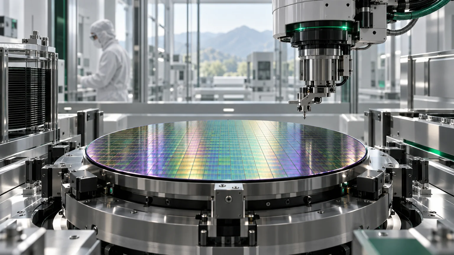
Four acres of cleanrooms
The 600,000-square-foot building houses nearly four acres of advanced cleanroom space, Applied Materials said in a statement distributed by GlobeNewswire on October 12. The company said capital spending is expected to scale over time to approximately $5 billion as customer projects begin.
Inside the centre, chipmakers, systems companies, equipment partners and university researchers will work alongside Applied's scientists and engineers to speed up chip innovation for AI, the company said.
Founding partners
TSMC, Intel, Samsung Electronics, Micron and SK hynix are founding partners, joined by Broadcom, Advantest, SCREEN, KIOXIA and Besi as innovation partners, according to the statement as reported by Semiconductor Digest. The goal is to develop materials, equipment and process technology in parallel rather than in sequence, shortening the path from research to high-volume manufacturing, Applied said.